


The core manufacturing technology of optical filters—optical coating process
Jan. 12, 2026
Optical filters have a wide range of applications in our daily lives—from smartphone cameras to high-end scientific instruments, from security monitoring equipment to medical diagnostic tools. These seemingly simple optical components rely on a precise and complex technology: optical coating. It is this technology that gives optical filters the ability to precisely control light, making them an indispensable core component of the modern optical industry.
Optical coating: the "soul" of a filter.
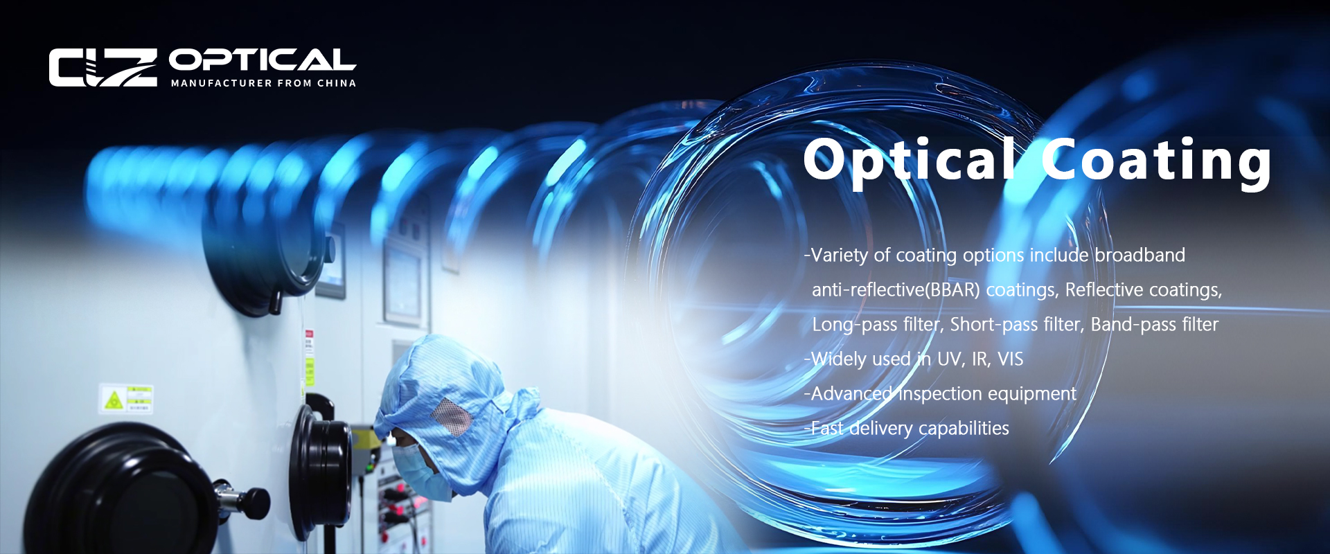
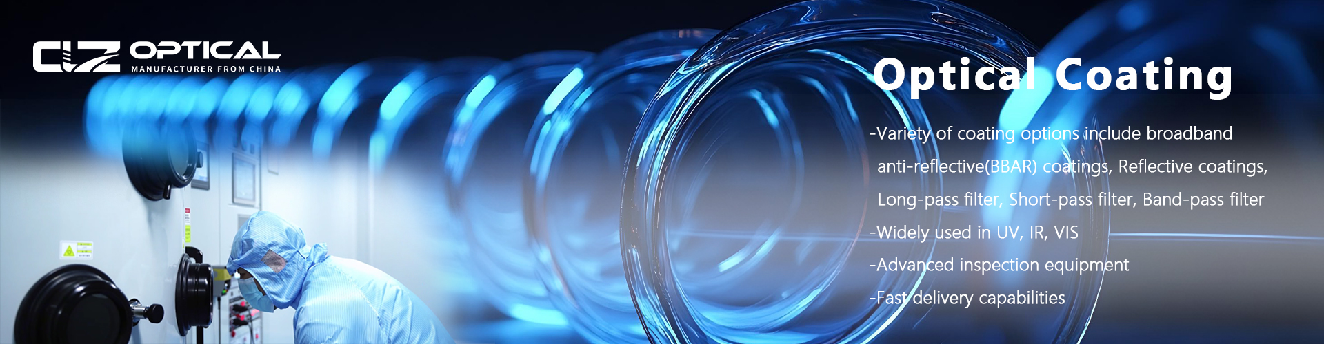
The fundamental function of an optical filter is to selectively transmit or reflect light of specific wavelengths as needed. The key to achieving this lies in the thin-film system covering its surface. These films are not simple coatings, but rather precisely designed multilayer structures, with the material and thickness of each layer carefully calculated to achieve specific optical properties.
The essence of optical coating technology is to deposit one or more thin films of specific materials onto the surface of a substrate. The thickness of these films is typically on the nanometer scale, equivalent to one-hundredth the diameter of a human hair. By controlling the thickness, number of layers, and materials of the films, the reflection and interference effects of light at the film interfaces can be precisely controlled, thereby achieving selective transmission or reflection of light of specific wavelengths.
Main methods of coating process
Currently, the mainstream coating technologies are mainly divided into two categories: physical vapor deposition and chemical vapor deposition.
1. Physical Vapor Deposition (PVD)
Vacuum evaporation is the most traditional and widely used technique in physical vapor deposition. In a high-vacuum environment, the deposition material is heated to evaporate or sublimate, causing it to deposit on the substrate surface in atomic or molecular form. This method has relatively simple equipment and is suitable for depositing films on most metals and dielectric materials. With technological advancements, improved techniques such as electron beam evaporation and ion beam-assisted deposition have improved the uniformity and density of the films.
Magnetron sputtering is another important PVD technique. An inert gas (usually argon) is filled into a vacuum chamber, and an electric field is applied to ionize the gas, generating plasma. Ions in the plasma bombard the target surface, ejecting target atoms and depositing them onto the substrate. This method offers high deposition rates and strong film adhesion, making it particularly suitable for preparing metal thin films and complex multilayer structures.
2. Chemical Vapor Deposition (CVD)
CVD technology generates solid thin films on a substrate surface through chemical reactions. A gaseous precursor containing the elements that make up the film is introduced into a reaction chamber, where a chemical reaction occurs on the substrate surface, depositing the film. CVD technology can obtain films with higher purity and density, but its equipment cost and process complexity are correspondingly higher.
Regardless of the technology used, modern coating processes rely heavily on sophisticated monitoring systems. Optical monitoring methods determine film thickness by measuring changes in the sample's transmittance or reflectance in real time during the coating process; quartz crystal monitoring methods indirectly estimate thickness by measuring changes in the mass of the film deposited on a quartz crystal. These monitoring technologies ensure that each film layer achieves the precise thickness required by the design.
The Science of Multilayer Film Design
A single thin film can only achieve limited optical effects, while modern filters typically employ multilayer film designs to achieve complex spectral properties through the interference and superposition of multiple light waves. The most common multilayer film structure is a periodically alternating high-refractive-index layer and a low-refractive-index layer; this structure is called a distributed Bragg mirror.
Designing such a multilayer film system requires solving a series of complex problems: How to select matching combinations of film layer materials? How to determine the optimal thickness of each layer? How to obtain a smooth transmittance curve over a wide wavelength range? How to ensure the film's performance is stable under oblique incidence? These problems require comprehensive optimization combining thin-film optics theory, materials science, and advanced algorithms.
Take the most common infrared cutoff filter as an example. It needs to maintain high transmittance in the visible light band (400-700 nm) while achieving high reflectivity in the near-infrared band (700-1100 nm). To achieve this goal, a film system with more than 30 layers is usually required, with the thickness of each layer precisely calculated. Such filters are widely used in smartphone cameras, ensuring that color image sensors are not affected by infrared light interference and achieve true color reproduction.
Process Challenges and Solutions
In actual production, the coating process faces numerous challenges. Film thickness uniformity is paramount, especially for large-size substrates. Solutions include improving the evaporation source layout, optimizing substrate rotation, and employing planetary rotating fixtures. Film stress control is also crucial; excessive stress can lead to film cracking or substrate deformation. Stress issues can be effectively mitigated by adjusting process parameters, using intermediate buffer layers, or performing post-annealing.
Environmental stability is a mandatory requirement for filters. The film needs to withstand temperature variations, humidity corrosion, and mechanical abrasion. Therefore, post-coating hardening treatment or deposition of a protective layer is typically required. For extreme environmental applications (such as aerospace or military fields), special properties such as radiation resistance and corrosion resistance must also be considered.
As optical filters become more complex and precise, coating processes are constantly innovating. Atomic layer deposition (ALD) technology enables sub-nanometer-level thickness control, making it particularly suitable for fabricating ultrathin filters. Plasma-enhanced chemical vapor deposition (PVD) combines the advantages of PVD and CVD, improving film quality and deposition rate.
Faced with ever-increasing technological demands, optical coating processes are developing in several key directions. First, uniform coating technology for larger substrates to meet the needs of large-size displays, photovoltaic panels, and other fields. Second, controllable fabrication technology for more complex film systems, such as aperiodic and graded refractive index films. Third, the development of novel coating materials, especially wide-bandgap materials and phase-change materials with special optical properties.
Intelligent manufacturing is another important trend. By introducing machine learning algorithms to optimize coating parameters, combined with real-time monitoring and big data analysis, precise control and fault prediction of the process can be achieved. This will greatly improve production efficiency and product consistency, and reduce production costs.
The development of tunable filters is of particular interest. Once a traditional filter is manufactured, its spectral characteristics remain fixed. Tunable filters based on liquid crystals, electrochromic materials, or microelectromechanical systems (MEMS) can have their optical properties altered by external electrical signals or mechanical adjustments. These filters hold great promise for applications in spectral imaging and adaptive optics, and they place entirely new demands on coating processes.